Breadcrumb
- Home
- Methodology
- Scanning Electron Microscopy
Scanning Electron Microscopy
Main navigation
Jump to backscattered electron imaging section.
When one decides to use electron microscopy to investigate a specimen, the end goal of the project must be evaluated to properly choose the right path to obtain that goal. Some applications where the scanning electron microscope would be the instrument of choice might be: studies involving the exterior morphology of the sample, the localization of large (10-30 nm) colloidal gold markers on the surface of the sample, the localization of boundaries between regions of differing atomic number composition, and the qualitative and quantitative identification of the elemental content of the specimen. Each of these applications requires that the instrument be operated properly to maximize the excitation and collection of the desired signal.

Most electron microscopes are high-vacuum instruments. Vacuums are needed to prevent electrical discharge in the gun assembly (arcing), and to allow the electrons to travel within the instrument unimpeded. There are many scales to measure vacuum levels, some being: mm/Hg, Pascals, Torr, and atmospheres. No matter the units used, if higher vacuum levels are desired, better pumping systems are required. Better systems cost more money. Why would one want better vacuums?
When designing the microscope, we started with the vacuum. The electron microscope source to be used should be a factor in the design of the vacuum system. Poor vacuum levels shorten the life of the electron emission source. Saving money in designing the vacuum system might prove costly if filaments are consistently in need of replacement. Also, any contaminants in the vacuum can be deposited upon the surface of the specimen as carbon. Cleaner vacuums will minimize this artifact.
Different electron emission sources require different vacuum levels. There are 2 classes of emission sources, thermionic emitters and field emitters. Thermionic emitters use an electrical current to heat up the filament which lowers the work function of the filament material. When the work function is lowered, electrons can be more readily drawn off the filament with an electric field. The two most common materials used for filaments are tungsten and lanthanum hexaboride. Cold cathode field emission sources do not heat the filament material. The electrons are drawn from field emission guns by placing the filament at a huge electrical potential gradient, so large that the work function of the material is overcome, and electrons are drawn off the filament. Field emission systems require extremely high, clean vacuums in which to operate.
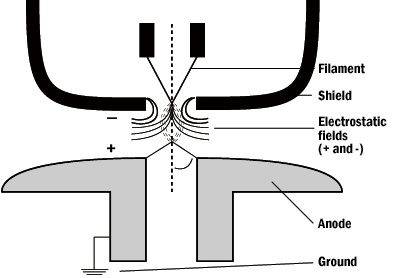
Field emission sources utilize two anode plates placed below the gun assembly. Associated with the first anode is the extraction voltage. The extraction voltage is usually in the range of 3-5 kilovolts and is the amount of voltage necessary to draw electrons from the source. The second anode has the accelerating voltage associated with it. The accelerating voltage determines the velocity at which the electrons travel down the column. Both anodes act as electrostatic lenses, focusing the beam into a small initial crossover.
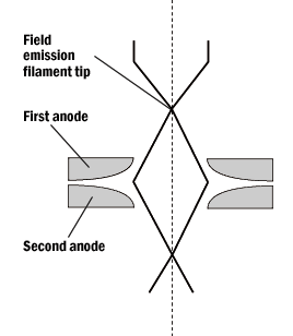
Two factors associated with the gun determine the resolution capability of the instrument. First, resolution must be defined. Resolution is the ability to separate (resolve) two closely spaced points (particles) as two separate entities. The two factors that determine resolution in the scanning electron microscope are accelerating voltage and initial crossover diameter.
Without getting into physics, we can generalize Abbe's equation as stating that the resolution of an instrument is dependent upon the wavelength of its illumination source. The accelerating voltage of a scanning electron microscope is variable, usually in the range 500-30,000 volts. An electron accelerated by a potential of 30Kv has a shorter wavelength than one accelerated by a 5Kv potential. Thus, the 30Kv electron should give us better point to point resolution. When we discuss specimen-beam interactions, we will contrast the difference between point to point resolution and surface resolution.
The other component of resolution, initial crossover (beam diameter) has many names. Some texts refer to it as the virtual source, others as do. To resolve a feature on the surface of a specimen, the beam must have a smaller diameter than that feature, yet still contain enough electrons (referred to as beam current density) to generate acceptable amounts of signal (to be discussed with specimen-beam interaction/signal formation). The smaller that the initial crossover is, the less that the electromagnetic lenses work to demagnify the beam into a usable probe. A thermionic system operating with a tungsten hairpin filament will have a crossover diameter of about 50 microns. A thermionic system equipped with LaB6 (lanthanum hexaboride) electron source will have a crossover of about 10nm, while maintaining high beam current densities (brightness). Without any subsequent focusing action of electromagnetic lenses, the field emitter has a probe that can be used for imaging purposes. This makes the field emission system the highest resolution instrument.
So why doesn't everyone use field emission SEMs? Cost and need. Not everyone can afford to purchase a FESEM. Also, there is the phenomenon of empty magnification. On some specimens, biological samples, as an example, there is a magnification that if exceeded, no useful information will be gained. The higher magnifications and resolutions of the FESEM is not always desired or required.
There is an inherent fluctuation of emission with the cold cathode FESEM. Any contaminants that come to rest on the filament cause the emission current to fluctuate. This prevents the FESEM from being interfaced with a quantitative microanalyzer, since a prerequisite of good quantitative analysis is a steady beam current.
FESEMs are extremely useful in low voltage applications. The design allows for coherent beam formation at low (500-3,000) voltages. FESEM technology has been used extensively by the semiconductor industry for quality control. An instrument that could check the progress of water fabrication without damage was needed. The FESEM operating at low voltages fit this niche.
So far, we have a vacuum and an electron beam generated and headed down the electron column. To assist us in the refinement of the electron beam, the electromagnetic lenses are employed.
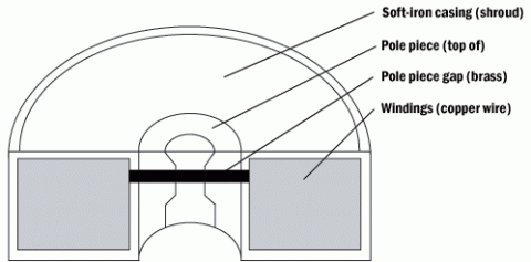
The path of an electron can be altered by exposure to a magnetic field. Electromagnetic lenses create a circular magnetic field that demagnify (condense) the electron beam as it passes through. The strength of the lenses can be changed by varying the current supplied to the lens. Changing the lens current affects the focal length of the lens.
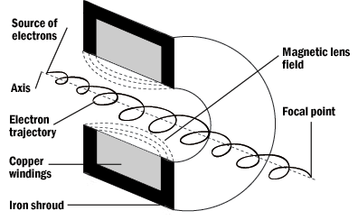
There are some problems inherent in electromagnetic lenses. They are spherical aberration, chromatic aberration, diffraction and astigmatism. It is possible to correct for these problems, once one understands them.
Spherical aberration concerns the path of the electron in respect to its position within the electromagnetic lens. The strength of the magnetic field is the strongest near the surface of the lens. Therefore, the electrons that travel through a lens close to its surface will have their paths altered more than an electron which travels through the center of the lens and results in a loss of electrons from the beam (electrons that strike the interior surface of the electron column are absorbed).
Chromatic aberration relates to the varying energy of the electrons that comprise the beam. Not all electrons generated at the gun assembly have the same energy. Electrons with different energies have different wavelengths. A magnetic field will have more of an influence on a longer wavelength electron. Thus, due to a variance in the energies of the electrons in the beam, it is not focused to a discrete focal point.
Diffraction is of most importance at the final probe forming lens. Diffraction is caused by the electron's wavelengths being out of phase. Thus, a lens will focus electrons of different phase to a different point depending upon the position of an electron in its wavelength when it passed through the lens. To correct diffraction, the electrons would have to be monochromatic and coherent. If these conditions were met, the lens could focus the stream of electrons to a point rather than to a disk of confusion.
Astigmatism occurs because of manufacturing imperfections within the electromagnetic lens. It is extremely difficult to manufacture an electromagnetic lens that forms a perfectly even magnetic field. Variances in the strength of the magnetic field around the circumference of the lens causes an elliptical focal spot. This problem can be overcome by segmenting the lens into many parts and being able to adjust the excitation to each part. In this manner, weak portions of the lens can be strengthened.
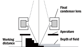
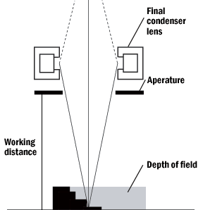
Along with the electromagnetic lenses, metal aperture strips can be used to refine the beam. It is common for the modern SEM to be equipped with variable condenser and objective lens apertures. These variable aperture strips will have a variety of pinhole sizes to choose from. It is the responsibility of the operator to choose the proper aperture size. To generalize, small objective aperture sizes will produce images with good resolution, good depth of field and minimal charging. This last statement requires two definitions. Depth of field refers to the ability to have a large change in specimen topography appear to remain in focus. SEMs allow for the specimen to be translated along the x, y and z axes. The z axis is defined as the distance from the final lens to the surface of the specimen. This distance is also referred to as the "working distance." Long working distances and small apertures provide an image that appears to be in focus over a large change in z. Having dealt with depth of field, a brief statement on charging is in order. An ideal specimen would be conductive. If a less than ideal (non-conductive) specimen is attempted to be viewed, beam electrons can build up on the surface of the specimen, resulting in the phenomenon known as charging. Charging will be further explained in specimen-beam interaction/image formation.
After the objective aperture, the last manipulation of the beam prior to impingement upon the sample occurs in the final lens. The final lens is the heart of the SEM and gives the instrument its name. Within the final lens are the raster coils. These coils raster or scan the focused electron beam over the surface of the specimen. Hence the name, scanning electron microscope. The raster coils scan the focused electron beam across the specimen much as one would read this page. You start at the top, read across the page to the end of the first line, drop down a line and back to the left and repeat. The scan of the raster coils is synchronized with the scan of the viewing screen. The raster coils are used to change magnification. To increase magnification, the coils can be made to scan a shorter line on the specimen. Since the size of the viewing CRT is fixed, the information generated by a shorter scan on the specimen must be enlarged to fill the viewing CRT. This is how magnification is changed.
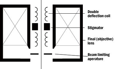
Now we have the beam converging on a point upon the surface of the specimen. This is focus. The true definition of working distance should state that it is the distance between the final lens and the specimen, when the specimen is in focus. Now is a good time to proceed into the specimen-beam interactions.
When the electron beam strikes the surface of the specimen, the primary (beam) electrons interact in either an elastic or inelastic fashion with atoms of the specimen. Elastic scattering events are those where the primary electron comes close to the nucleus alters the path of the primary electron with a minimal loss in electron velocity.
Backscattered electrons will have an energy range from 50eV (electron volts) up to the accelerating potential the SEM is being operated at. Elastic scattering can change the path of the primary electron up to 180 degrees. A primary electron whose path is altered enough to have it leave the specimen is referred to as a backscattered electron. The amount of backscattered electrons emitted from a specimen is dependent upon the atomic number of the specimen. This is known as the backscattered coefficient, and as a general rule, the number of backscattered electrons emitted from a specimen increases with an increasing atomic number. Also, increasing the beam current will excite more backscattered electrons from the specimen. With proper detector, the image formed from the backscattered electrons emitted from a specimen will show regions of atomic number inhomogeneity.
Inelastic events are those where the primary beam electron has a collision with a nucleus or electron of an atom of the specimen. The primary electron undergoes a change in direction, as well as transferring energy to the specimen. Some signals generated by inelastic events are: auger electrons, secondary electron, characteristic x-rays and bremsstrahlung radiation. Auger electrons are used to characterize the elemental composition of the surface of a specimen. Characteristic x-rays can be collected and sorted to provide elemental information of the specimen. For this lecture, the signal of most importance is secondary electrons.
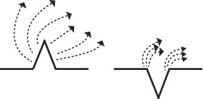
A secondary electron is an electron of an atom of the specimen that has been knocked from its orbit. The energy range for secondary electrons states that the electron must have an energy greater than the 0eV but less than 50eV. This energy range limits the depth from within the specimen which the electron can escape. The energy range also produces what is referred to as the edge effect. Edges of the specimen provide greater amounts of surface area from which the weak secondary electrons can escape. Thus, at the edges of features on the specimen, more secondary electrons are emitted. These areas appear brighter in the image.
The group of secondary electrons (SE) can be divided further. There are SEI, SEII, SEIII, and SEIV. These electrons are classed according to how they are generated. A SEI is an electron is an electron that is generated at the point of primary beam impingement in surface of the specimen. Thus, it carries the highest resolution information. A SEII is an electron that is generated when a backscattered electron leaves the surface of the specimen. Due to the energy of backscattered electrons, this SEII could leave the surface of the specimen microns away from the primary beam impingement site. SEIIs hurt the resolution of the image but add greatly to overall image brightness. A SEII is an electron released when an energetic backscattered electron strikes the interior of the specimen chamber, causing a SE to be released. SEIVs are formed when the primary beam strikes an aperture within the electron column. SEIIIs and SEIVs contribute noise to the image. By understanding signal formation, the specimen can be properly prepared for analysis.
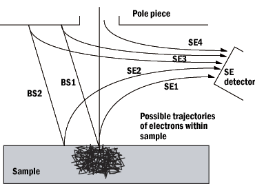
Since secondary electrons are weak (less than 50 eV, their trajectories can be bent toward a detector that has a positively biased grid in front of it. The most commonly used detector is the Everhart/Thornley design.
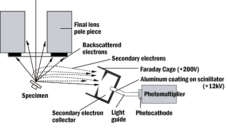
When the secondary electron strikes the face (scintillator) of the detector, the electrical energy is converted to a photon. The photon travels down a light pipe, where it enters the photomultiplier tube. In the photomultiplier tube, the photons are changed back to electrical energy, undergoing cascading events across a series of dynodes to enrich the signal. The signal is further refined in the preamplifier and amplifier before being projected onto the screen of the viewing cathode ray tube. There is a one-to-one correspondence between a point scanned on the sample, and a pixel on the viewing screen.
When a sample is to be prepared for examination at the SEM level, there are a few things one must keep in mind. The most important being that the sample must remain in as unaltered state as possible for valuable information to be gained. This is not always possible, especially with samples that are not electrically conductive. Why is conductivity important?
The design of the SEM is that the specimen stage is at ground potential. It is hoped that the primary electron beam is absorbed by the specimen, and then this current is dissipated through the stage. Failure of the current to dissipate results in specimen charging, which at the least, makes imaging difficult. Therefore, there should be a conductive path from the point of beam impingement, through the specimen, specimen mount, and finally specimen stage.
Preparation can be divided into three steps:
- Specimen selection and preparation
- Specimen mounting
- Specimen coating.
Specimen selection involves the acquisition /production of a sample. The sample selected must be representative of the entire group if data is to be extrapolated to the entire population. For biological specimens, the method of preparation is very similar to the methods employed for TEM. Primary fixation is routinely carried out making use of aldehydes. Paraformaldehyde, glutaraldehyde, or mixtures of these two can be used to cross-link the proteins in the sample. After primary fixation, a secondary fixation using osmium tetroxide is performed. This stabilizes some fats and lipids within the sample. Dehydration through a graded series of ethanol removes the water from the sample. To remove ethanol from the sample, it can either be critical point dried, or chemically dried with hexamethyldisilizane (HMDS). Preventing the gas/liquid interface is the main goal of critical point drying (as well as the alternative process of HMDS). Whenever a liquid evaporates into the gaseous phase, large surface tension phenomena occur. These surface tensions can harm fine surface details on the surface of the sample. Since the SEM is a surface imaging technique, it is desirable to avoid such artifacts. For critical point drying, the samples are loaded into the chamber of a critical point drying apparatus. This chamber is surrounded by a water jacket that allows the operator to vary the temperature of the unit. Initially, the chamber is cooled below 13° Celsius. At this temperature, liquid carbon dioxide will flow into the chamber, and remain in the liquid state. Ethanol is denser than liquid carbon dioxide, and will flow out of the specimen, to the bottom of the chamber. There are ports in the bottom of the chamber that allow the operator to purge away the ethanol. When all of the ethanol has been purged away, the level of liquid carbon dioxide in the chamber is lowered (prevents high pressures from being attained), and the chamber is heated above 31° Celsius. The "critical point" of carbon dioxide is approximately 31° Celsius and 1070 lbs/square inch. At this pressure and temperature, carbon dioxide wants to exist as both a liquid and a gas. In this state, the carbon dioxide can be purged off, preventing the gas/liquid interface. Critical point drying usually provides the best sample preservation but can take up to 3 hours to perform. Using HMDS instead of critical point drying is quicker and can yield acceptable results on some samples. When the sample is dehydrated to 100% ethanol, a fifty/fifty mix of ethanol/HMDS can be placed on the sample followed by 2 or 3 exchanges of HMDS. After these exchanges, sample is in a fume hood where HMDS evaporates off. The vapor pressure of HMDS is such that surface damage is minimal. The results of using HMDS vary, so it’s best to experiment with both drying techniques.
The outline above is a commonly followed protocol. For some samples, a tannic acid step might provide added rigidity to the cells. Tannic acid can be mixed with the primary fixative or can be placed in the 70% ethanol step. A 1% solution of tannic acid is the most common, but this can be varied. Another method of adding mechanical stability, along with increased electron density, is the O-T-O method. The O-T-O method refers to the use of a thiocarbohydrazide step between two osmium exposures. The thiocarbohydrazide acts as a mordant, meaning that it forms a "bridge" between two layers of osmium. Samples prepared in this fashion yield increased amounts of secondary electrons, thus providing images of higher-quality.
For material science samples, specimen preparation must initially involve desiccation. The specimen must have all volatile materials removed from it so as to not degrade the vacuum of the SEM. Once dry, preparation may proceed, and may take many forms. A few would be: ion milling, heating/baking, epoxy embedment, ashing and etching (acid/base). The information desired from the specimen will dictate which preparation approach to take. For example, the best quantitative x-ray information is collected from a specimen with a flat surface. This is due to the possibility of surface protrusions absorbing x-rays before they reach the x-ray detector. This is known as shadowing. To prevent this, specimens for quantitative x-ray microanalysis should be polished flat. Once the specimen is prepared, it next needs to be mounted.
A variety of specimen mounts are commercially manufactured. The brand of SEM you are going to utilize determines which style to use. The Hitachi SEMs require the use of Cambridge style stubs (in our lab, there are several microscope stages available, so the use of the Cambridge style stub is not mandatory, but most common).
The specimen stubs most commonly used are made up of carbon or aluminum. If x-ray information is desired of the specimen, it might be wise to select a carbon stub to minimize confusing elemental lines in the x-ray spectra. It should be noted that these carbon stubs are rather expensive ($5 each), but if a specimen is thick enough to prevent beam penetration, their use may be necessary. Once the stub is selected, the attachment of the specimen to the stage is the next consideration. Common adhesives include: colloidal silver or carbon, carbon/copper/aluminum tapes, double-stick tape, super glue, and epoxy resins. Some of these are better conductors than others, while others may contribute to elemental background. Adhesives must be thoroughly outgassed before the specimen is introduced into the SEM. Failure to do so will lead to specimen hydrocarbons on the surface of the specimen. This contamination build-up can mask fine structural details. Specimen outgassing will also degrade the resolution of the instrument.
Specimen coating, if necessary, follows specimen mounting. If the specimen is conductive, it might not require coating. If x-ray microanalysis is to be performed, the evaporation of a carbon film over the specimen will render it conductive without introducing cluttering elemental lines to the spectra. The carbon deposition should be minimal, just enough to create conductivity without absorbing weak x-rays that leave the specimen. Carbon coatings are also useful when backscattered images are desired.
Metallic coatings can be used to boost the secondary electron emission of the specimen as well as rendering it conductive. Aluminum, gold, platinum, chromium, tungsten, tantalum, and palladium are common metals used to coat specimens. The two most common methods of coating are thermal evaporation and sputter coating. With thermal evaporation, there is the risk of radiant thermal damage to the specimen. Also, the metallic particles may retain enough heat to burn into the specimen. Sputter coating is generally the preferred method of specimen coating. Sputter coating takes place in a vacuum chamber. The specimen to be coated is loaded upon the anode. A vacuum is generated. Prior to coating, the vacuum is compromised with an inert gas (usually argon). When a high tension is applied to the cathode where the metal source resides, the argon gas molecules are attracted to the cathode. The ionized argon strikes the metallic target, knocking loose metal grains, which are attracted to the anode. Due to the directional randomness of the argon/target collisions, an omnidirectional coating is achieved upon the specimen.
There is discussion in the literature about coating vs. decoration. Sputter coating of gold and gold/palladium mixtures is referred to as decoration. When a metal grain from such a source strikes the surface of a specimen, it is mobile creating islands of coating. Metals such as chromium, tantalum, and tungsten tend to stick where they land upon the surface of the specimen. Therefore, they are classified as coatings.s.
Grain size of the metal produced is also important. Smaller grains provide better resolution. This is because they obscure less specimen detail. Au and Au/Pd grain sizes are about 2-2.5 nanometers. Cr and W can produce grain sizes on the order of 0.5 nanometers. Thus, Cr and W coatings can generate higher resolution images. A drawback to Cr and W is that the equipment needed for their use can be expensive. Also, Cr coatings readily oxidize. Iridium can be used in place of Cr and W.
In the discussion of signal generation, it was stated that the number of backscattered electrons increases with increasing atomic number. It was also stated that the BSE signal lacks high-resolution information. From these two statements, what can be predicted about gold vs. chromium coatings? Chromium, having a lower atomic number than gold, generates fewer backscattered electrons. This makes it a better coating for high-magnification use. It takes a special field emission (in the lens) SEM to resolve the coating grains. The average SEM cannot take advantage of the increased resolution of the Cr coat.
Once prepared, the sample should be stored in a vacuum desiccator. This prevents hydration to atmospheric humidity levels and reduces oxidation of the metal coating. Most specimens can be stored indefinitely with little appreciable degradation.